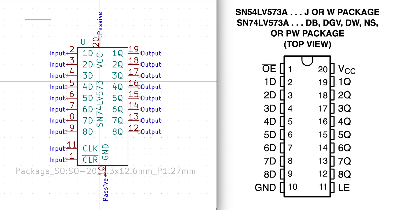
20+ d flip flop block diagram
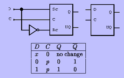
We know that one flip-flop can store one-bit of information. D Flip Flop DFF with asynchronous preset and clear timing diagram.
![]()
A Pulse Sequence For Nmr Spectroscopy And Nuclear Rabi Oscillations Download Scientific Diagram
Develop a table showing the state for 20 clock pulses.

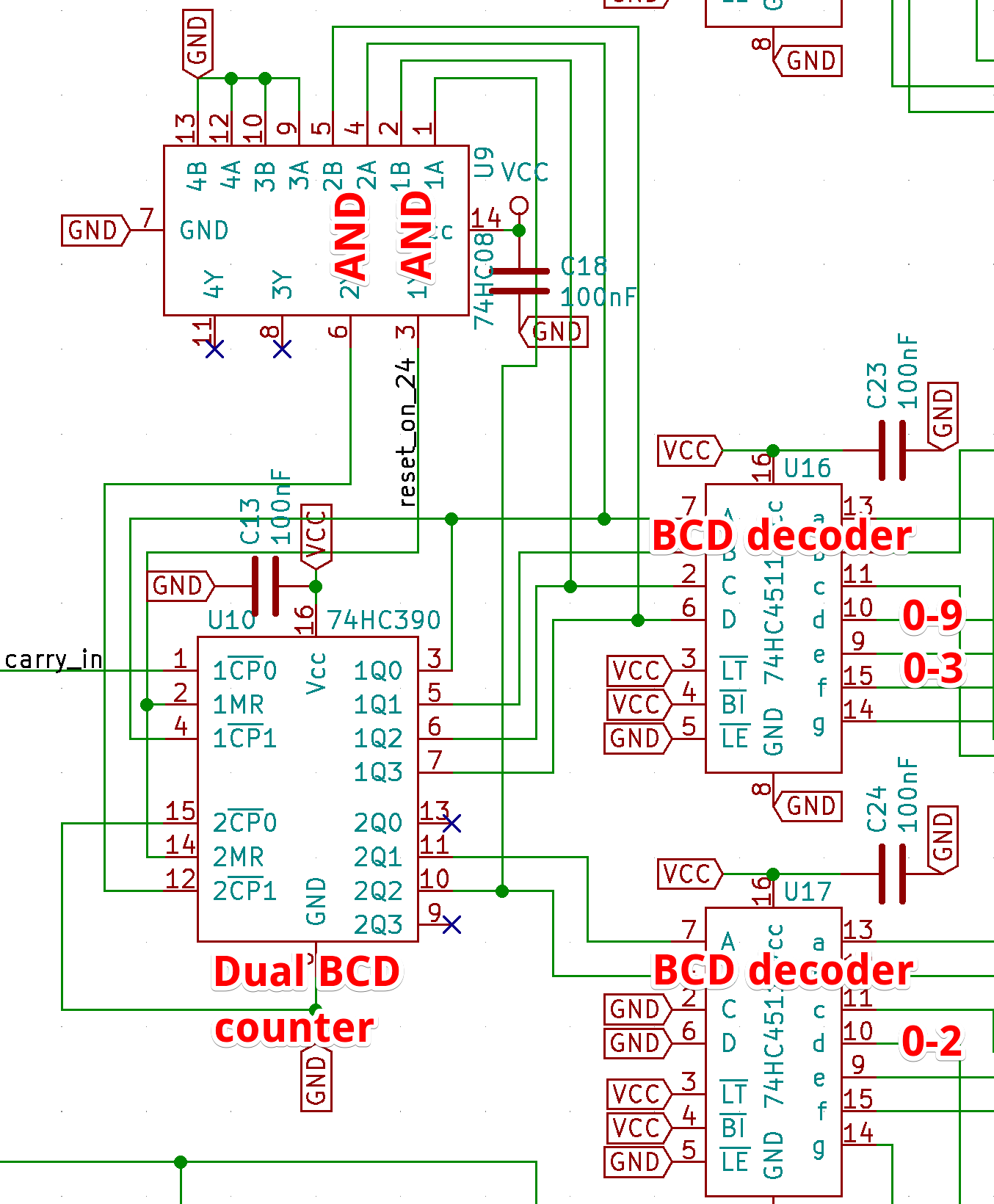
. 20 The block diagram of a positive-edge-triggered D flip-flop is shown in Figure 1. Whenever the clock signal. The S and R inputs of the RS bistable have been replaced by the two inputs called the J and K input respectively.
The major applications of T flip-flop are counters and control circuits. A T flip-flop is a modified form of the JK flip flop. Block diagram of a D flip-flop 2.
Implement a two-input AND gate shown in Figure 2a with. The circuit diagram of the J-K Flip-flop is shown in fig2. D flip flop are also known as a Delay flip flop or Data flip flop.
The circuit diagram of the JK Flip Flop is shown in the figure below. D flip flop can only store 1 bit binary data. The circuit diagram of D flip-flop is shown in the following figure.
Posted on November 23 2021. This circuit has single input D and two outputs Qt Qt. T flip flop is modified form of JK flip-flop making it to operate in toggling region.
The operation of D flip-flop is similar to D Latch. Draw the block diagram for a 4-bit ripple counter using D Flip-Flops. Draw the block diagram for a 4-bit ripple counter using D.
It is advance version of SET and. Operation using11 instructions are. Here J S.
20 The block diagram of a positive-edge-triggered D flip-flop is shown in Figure 1. It is the drawback of the SR flip flop. 140 Lectures 20 hours.
In order to store multiple bits of information we require multiple flip-flops. The S and R inputs of the RS bistable have been replaced by the two inputs called the J and K input respectively. In SR NAND Gate Bistable circuit the undefined input condition of SET 0 and RESET 0 is forbidden.

20 Job 2 Process Jsp Instance Considered In This Work And Its Optimal Download High Resolution Scientific Diagram
2
2
![]()
Schematic Diagram Of A Conventional D Flip Flop Download Scientific Diagram

Hedging Strategy For An American Put Option With Strike 20 And S 0 20 Download Scientific Diagram

Cholesterol Distribution In Small Unilamellar Vesicles The Journal Of Physical Chemistry B

1 Basic Signal Processing System 13 Download Scientific Diagram

Heterologous Protein Expression In The Shake Flask Condition Identified Download Scientific Diagram
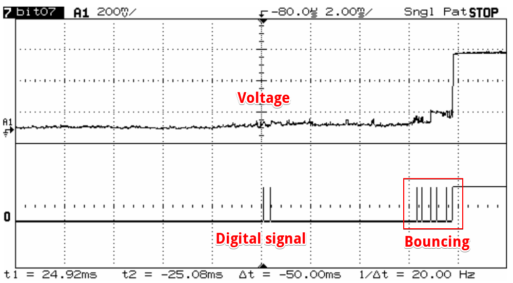
A Digital Quartz Clock From Scratch By Erik Van Zijst Medium
Reprinted From Bonsiepe G Maldonado T 1963 Zeichensystem Fur Download Scientific Diagram

Oops I Went Home For Christmas How To Readjust To Life Abroad After A Quick Trip Home The Culture Blend
A Digital Quartz Clock From Scratch By Erik Van Zijst Medium
Diy 8 Bit Handheld Multiplayer Gaming Device Medium
Flip Flop Circuit Types And Its Applications

Learn How To Make A Lighthouse And An Electric Circuit At Stimix Educrafts Projects For Kids Science Projects Circuit Projects

Block Diagram Of The Receive Path For The Ettus Research Wbx Rf Download Scientific Diagram
Timing Error Aware Microcontroller Springerlink